During a board bring-up process, it is very important to check the connectivity from various pins from the chosen SoC to various components of your board. One of the first things done as part of the board bring-up/boot process is toggling the reset lines of different ICs present on the board. These ICs may be as simple as a temperature sensor or complex as an RF transceiver. Reset pins of these chips are usually connected to a dedicated pin on the SoC. The application processor/DSP on the SoC runs the bulk of the software of the product.
Some designs keep it simple and have dedicated SoC pins connected to reset lines, while others may try to conserve the SoC pins and use Decoder/Demultiplexer ICs, like [1] SN74LS138, for controlling reset pins instead. I am personally not a board designer and not an expert on these design decisions, but most of the boards I have worked with keep it simple!
I will use the most recent SoC I have been working on, [2] AM5728 from TI, to practically explain the core topic of the blog, how to toggle a GPIO pin!
There are a few important steps to follow before we get our Oscilloscope out to probe the test points on the board.
- Have the schematics of the board handy with you
- Check the SoC pin/ball number as mentioned in schematics against the pinmux configuration in the datasheet. Simple microcontrollers like [3] ATmega328P (seen in Arduino Uno board) have dedicated GPIO pins and do not need [4] Pinmux programming for selecting functionalities on their pins
As an example, I will use GPIO Bank-4, Pin-0 in AM5728, and show how this pin can be toggled from different software and cores during board bring-up. We will talk about four different places from where the said GPIO pin can be toggled,
- Uboot using md and mw commands
- Linux using devmem commands
- Linux (again) using GPIO sysfs entries and Devicetree
- SysBios using direct register commands
The first three in the above list run from Cortex A15 and the last one runs on the C66x DSP core of AM5728.
Below steps are the common programming steps to be carried out on the SoC. We will show using different commands how this can be achieved.
The first important thing to do is to select the GPIO 4.0 functionality by programming in the PinMux register. This feature of the SoC allows the application to use the G6 pin of the SoC to be used for any allowed functionality without any hardware changes. In our case, PinMux module register CTRL_CORE_PAD_VIN2A_VSYNC0 @ 0x4A003564 provides the below functionalities,
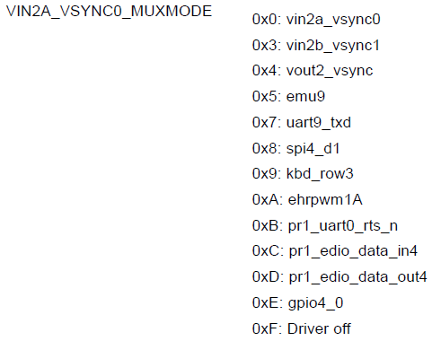

We are going to use the GPIO4.0 functionality by programming 0xE. There are other fields like Pullup-enable, Receive mode on the Pin, etc, and we are leaving the default values as these are sufficient for using GPIO4.0 as GPIO output.
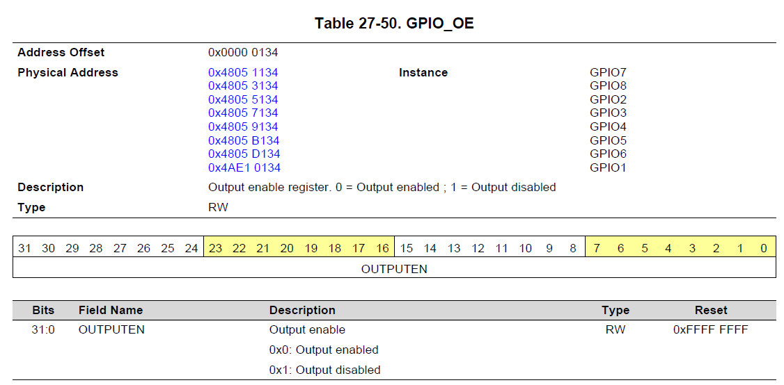
The second register programming to be done is to enable the Output functionality on the GPIO pin from the GPIO module. As we are only interested in toggling the Pin, we should clear the bit-0 of register GPIO_OE @ 0x4805D134. Refer to the [5] AM5728 TRM snippet below.
Finally, setting OR clearing bit-0 of GPIO_DATAOUT @ 0x4805D13C will drive the Pin/Ball G6 on the SoC to high (3.3V) or low (Gnd). Refer to the TRM snippet below.

Now coming to the specific programming commands.
U-boot using md and mw commands
Type in ‘help md’ or ‘help mw’ on U-boot prompt for its usage.
=> mw.l 0x4A003564 0xE 1
The below command is for setting the GPIO pin to the output function,
=> mw.l 0x4805D134 0x1 1
The below command gives High logic (3.3V) on the G6 SoC Pin,
=> mw.l 0x4805D13C 0x1 1
The below command gives Low logic (0V) on the G6 SoC Pin,
=> mw.l 0x4805D13C 0x1 0
Using the md command allows you to read back what has been written and can be used as in the below example. Please note, that a different address has been shown in the example below.
Linux using devmem commands
Using this command is similar to using md/mw commands.
The below command is for pin muxing the G6 SoC pin,
root@am572x-phycore-rdk:~ devmem2 0x4A003564 w 0xE
The below command is for setting the GPIO pin to the output function,
root@am572x-phycore-rdk:~ devmem2 0x4805D134 w 0x1
The below command gives High logic (3.3V) on the G6 SoC Pin,
root@am572x-phycore-rdk:~ devmem2 0x4805D13C w 0x1
The below command gives Low logic (0V) on the G6 SoC Pin,
root@am572x-phycore-rdk:~ devmem2 0x4805D13C w 0x1
Reading back using the command is more simple. Please note, that a different address is being read out in the below example.
SysBios using direct register access
This method requires us to write a simple C program, build it in CCS (Code Composer Studio) as a standalone program, and load it either using JTAG or from ARM. Regardless, once the DSP code is loaded and the main() execution starts, below is the routine we want to execute on the C66x core.
Register access can also be done using PDK-provided macros like, HW_WR_REG32() for write and HW_RD_REG32() for read. These are just for abstracting/simplifying the code and the below routine provides just the same functionality.
/** Routine to toggle output of GPIO pin G6 **/
void toggle_G6_gpio()
{
volatile uint32_t *reg_CTRL_CORE_PAD_VIN2A_VSYNC0 = 0x4A003564;
volatile uint32_t *reg_GPIO_OE = 0x4805D134;
volatile uint32_t *reg_GPIO_DATAOUT = 0x4805D13C;
*reg_CTRL_CORE_PAD_VIN2A_VSYNC0 = 0xE;
*reg_GPIO_OE = 0x1;
while (1) {
Task_sleep(1);
*reg_GPIO_DATAOUT = 0x1;
Task_sleep(1);
*reg_GPIO_DATAOUT = 0x0;
}
}
Linux (again) using sysfs entries and Device-tree
This part is a little more involved than the first three methods that were described. But is the preferred method of operation once you want your application to start controlling the GPIO lines. We will need to split the work into two sections, first, add appropriate entries in the device tree of Linux for proper pin muxing of the selected pin, ie, updating CTRL_CORE_PAD_VIN2A_VSYNC0 register is to be done from Device-tree, and second, using sysfs entries to program the GPIO pin.
First, the below entry should be added as part of an active pinmux configuration in Device-tree,
gpio_pins_defaults: gpio_pins_defaults {
pinctrl-single,pins = <
0x164 (MUX_MODE14) /* vin2a_vsync0.gpio4_0 */
>;
};
Value of 0x164 is offset from 0x1400 that is the address offset of CTRL_MODULE_CORE
(MUX_MODE14) macro selects the Mode-14, ie, gpio4_0 pin mux functionality of G6 pin
The second part of the programming involves using sysfs entries under /sys/class/gpio to toggle the GPIO pin. Before we proceed, we should first check if the GPIO entry is free and not being used already by some other driver. Below is how we can quickly check this,

GPIO Bank-4 – Pin-0, corresponds to gpiochip3,gpio-96. We see that entry is not present and in the GPIO subsystem, this Pin is free.
Now to do some setup operations to enable GPIO-4, Pin-0 in /sys/class/gpio. Below are the steps to do that,
You can see that after pin-96 was exported and the direction was set to ‘out’, the default value readout on gpio96/value is 0.
Now to toggle the output value is as simple as below,
Please note
- A simple addition of ‘gpio_pins_defaults’ entry in device tree is not sufficient. This pin-mux entry needs to be part of an active device-tree node for this entry to take effect
- Missing entry on ‘/sys/kernel/debug/gpio’ does not always mean, pin is free. It is always possible to bypass the GPIO subsystem and still use GPIO pins. This is out of scope from my current blog
- Support for using ‘/sys/class/gpio’ is coupled with GPIO driver that internally programs the same registers as seen in the first three methods
From the above four ways of toggling the GPIO-4; Pin-0, below are a few takeaways,
- Different cores on the SoC can control the state of the GPIO pins. But while any core can change/toggle the state of the GPIO pin, most of the time, the Master Core is responsible for programming the Pinmux functionality of the SoC pin
- Programming steps for using the functionality on SoC do not change, regardless of the software or the core being used
- The importance of Hardware-Software Interface (HSI) and Hardware-Abstraction Layer (HAL) is underlined with the fourth option, where enough abstraction is provided by the Linux GPIO subsystem and applications are made independent of the Hardware programming details
I hope this information helps in your current or upcoming projects.
Cheers!
References
[1] 3-line to 8-line decoder / demultiplexer
SN74LS138 data sheet, product information and support | TI.com
[2] Sitara processor: dual Arm Cortex-A15 & dual DSP, multimedia
AM5728 data sheet, product information and support | TI.com
[3] ATmega328P: Product site
ATmega328P – 8-bit AVR Microcontrollers
[4] Data sheet for ATmega328P
ATmega328P
[5] Technical Reference Manual (TRM) for AM5728
AM572x Sitara Processor Technical Reference Manual (Rev. L)
